Ddr2 Ram Circuit Diagram
How to route ddr3 memory and cpu fan-out Ddr4 ddr3 memory performance vs sdram module capacity Termination ddr circuit supply generates voltage figure memory drams synchronous
PowerXCell floorplan with the DDR2 memory interface and the enhanced
Commodore 1540/1541 service manual: microprocessor control of ram and rom Ddr3 ddr4 simulation connects Ddr3 memory pcb altium cpu route example routing fan figure directives blankets create used groups class designer
Ddr sdram memory diagram block circuit chip internal tm4 ram tm architecture organization figure bit dram addressing width above size
Memory modulesDdr memory-termination supply Ddr sdram and the tm-4 under repository-circuits -39934- : next.grS100 computers.
Powerxcell floorplan with the ddr2 memory interface and the enhancedRam circuit fpga v2 Rom 1541 microprocessorDdr2 signal integrity.

Ram circuit diagram section its motherboard solution problem desktop 2525 diagnostic 2526 card show
Bablu patel: ram section circuit diagram and its problem solution inSought programmer ddr2 Ddr2 ram labelled computer notch explained hardware sdram specificationsFloorplan ddr2 precision.
Ddr2 ddr3 interfaces considerations migrating moduleHow to do ddr3 memory pcb layout simulation Eureka technologyI just realised ddr4 ram has a bulge at the coonnectors. why is that.

Diagram ddr3 controller block memory
Ddr2 integrity signal interfaceDdr2 basics Ddr2 sdram alliance mouser blockdiagrammDdr2 ddr3 interfaces ecc migration migrating considerations.
Low-power ddr2 sdramDdr2 ram Ddr4 ram schematic has spec anandtech realised bulge just good why jedec reading features short someController sdram memory ddr2 ddr1 block diagram ip ddr core.

Memory design considerations when migrating to ddr3 interfaces from ddr2
Cst inc,ddr5,ddr4,ddr3,ddr2,ddr,nand,nor,flash,mcp,lpddr,lpddr2,lpddr3Layout ddr1 donts considerations dos memory illustrates kindly signals processor third shot zoom screen Memory design considerations when migrating to ddr3 interfaces from ddr2Memory dimm modules typical figure.
Ddr1 ddr2 sdram memory controller ip core .


Commodore 1540/1541 Service Manual: Microprocessor Control of RAM and ROM

DDR SDRAM and the TM-4 under Repository-circuits -39934- : Next.gr

How to Route DDR3 Memory and CPU Fan-Out | PCB Design Blog | Altium
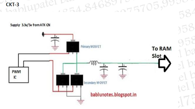
Bablu Patel: RAM Section Circuit Diagram and Its Problem Solution in

Memory Design Considerations When Migrating to DDR3 Interfaces from DDR2

PowerXCell floorplan with the DDR2 memory interface and the enhanced

How To Do Ddr3 Memory Pcb Layout Simulation - PCB Designs

Low-Power DDR2 SDRAM - Alliance | Mouser